
Table Of Contents
- Introduction: The Semiconductor Industry’s Seismic Shift
- A Landmark Deal: Unpacking Google’s Massive 3 Million TPU Order with Intel
- The Secret Sauce: Why Intel’s Advanced Packaging is a Game-Changer
- NVIDIA’s Strategic Pivot: Evaluating Intel’s 18A Process for Next-Gen GPUs
- The New Foundry Landscape: Intel’s ‘Coopetition’ with TSMC and Samsung
- Intel’s Foundry Roadmap: Key Technologies Driving the Comeback
- Foundry Titans Compared: Intel vs. TSMC vs. Samsung
- Key Takeaways
- Frequently Asked Questions
- Conclusion: A New Era for Semiconductor Manufacturing
Introduction: The Semiconductor Industry’s Seismic Shift
The global technology landscape is being fundamentally reshaped by the insatiable demand for artificial intelligence. From large language models to autonomous driving, the computational power required to train and run these complex systems is growing at an exponential rate. At the heart of this revolution are highly specialized semiconductors—the GPUs, TPUs, and AI accelerators that serve as the silicon brains of the modern world. For years, this critical manufacturing landscape has been dominated by a single titan: Taiwan Semiconductor Manufacturing Company (TSMC). However, the sheer scale of the AI boom is creating unprecedented capacity constraints and pushing the world’s largest tech companies to seek a more resilient, diversified supply chain. Amid this industry-wide scramble, a legacy giant is staging a remarkable comeback. Intel, under its revitalized Intel Foundry division, is rapidly emerging as a formidable alternative, securing monumental deals and evaluations from the very titans of AI that have long relied on its rivals.
Recent reports, citing sources from The Information and Reuters, have sent shockwaves through the industry. Google, the search and AI behemoth, has reportedly placed a massive order with Intel for over 3 million of its custom Tensor Processing Units (TPUs) to be delivered through 2028. Simultaneously, NVIDIA, the undisputed leader in AI accelerators, is actively evaluating Intel’s cutting-edge 18A process node and advanced packaging technologies for a future multi-die GPU design. These developments are not isolated wins; they are powerful validation points for Intel’s ambitious IDM 2.0 strategy and signal a potential tectonic shift in the high-stakes world of semiconductor fabrication. This article delves deep into the specifics of these deals, explores the underlying technologies that make Intel an attractive partner, and analyzes the broader implications for the competitive foundry landscape.
A Landmark Deal: Unpacking Google’s Massive 3 Million TPU Order with Intel
For years, Google has been at the forefront of developing custom silicon to accelerate its AI workloads. Its Tensor Processing Units (TPUs) are the engine behind many of its core services, from Search and Photos to its expansive Google Cloud AI offerings. To secure the sheer volume of chips required to maintain its competitive edge, Google has historically relied on a select few manufacturing partners. The news that it has now tapped Intel for a significant portion of its future TPU production is a watershed moment for Intel Foundry.
According to reports citing Morgan Stanley estimates, Google is projected to produce over 6 million TPUs between 2027 and 2028. The reported Intel order for over 3 million units through 2028 suggests that Intel could be responsible for manufacturing roughly half of Google’s entire TPU output in that final year. This is not a trial run or a small-scale experiment; it is a strategic, high-volume commitment from one of the world’s most influential technology companies. The decision to award such a substantial contract to Intel was not made lightly. It reportedly followed an extensive and rigorous validation process, where Google’s engineers closely scrutinized Intel’s advanced packaging capabilities, yield rates, and overall manufacturing readiness.
The significance of this partnership extends beyond the sheer numbers. It serves as a powerful endorsement of Intel’s technological roadmap and its ability to execute at scale. For a hyperscaler like Google, supply chain diversification is paramount. Over-reliance on a single foundry, even one as reliable as TSMC, introduces significant geopolitical and logistical risks. By bringing Intel into its manufacturing fold, Google not only mitigates these risks but also fosters a more competitive foundry market, which can lead to better pricing, more innovation, and greater access to leading-edge capacity. This deal validates Intel’s multi-billion-dollar investment in new fabs and technologies, signaling to the rest of the market that a credible, US-based alternative to Asian foundries is finally ready for prime time.
The Secret Sauce: Why Intel’s Advanced Packaging is a Game-Changer
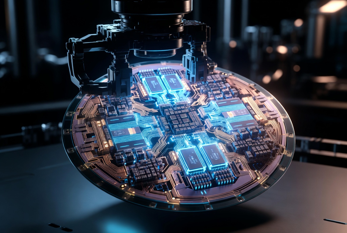
While cutting-edge process nodes like 18A (1.8-nanometer class) grab headlines, the unsung hero of modern chip design is advanced packaging. As traditional Moore’s Law scaling becomes more complex and expensive, chipmakers are increasingly turning to “chiplet” or multi-die architectures. Instead of creating one large, monolithic chip, designers create several smaller, specialized dies (chiplets) and integrate them into a single package. This approach improves yield, lowers costs, and allows for mixing and matching different process technologies. However, connecting these chiplets requires sophisticated interconnect technology, and this is where Intel has cultivated a significant competitive advantage.
A key technology driving the Google deal is Intel’s EMIB (Embedded Multi-die Interconnect Bridge). EMIB is an elegant and cost-effective solution for providing high-bandwidth, low-latency connections between chiplets. Unlike other methods that require a large silicon interposer, EMIB uses small, localized silicon bridges embedded within the package substrate, dramatically simplifying the manufacturing process. According to reports from Wccftech, Intel’s EMIB technology has achieved impressive yield levels of around 90%—a critical metric for high-volume manufacturing that undoubtedly caught Google’s attention. High yields translate directly to lower costs and more reliable supply, two factors that are non-negotiable for a company operating at Google’s scale.
The reports specifically suggest that Google’s upcoming TPU v8e, expected in the second half of 2027, is a prime candidate for incorporating Intel’s EMIB technology. This indicates that the partnership is not just about raw wafer fabrication but about leveraging Intel’s holistic “systems foundry” approach, where packaging is a core and integrated part of the value proposition. By offering a world-class packaging solution alongside its process nodes, Intel provides a one-stop-shop that simplifies the design and manufacturing process for complex, multi-die AI accelerators. This capability is a powerful differentiator that has not only attracted Google but has also drawn interest from other tech giants like Meta Platforms.
NVIDIA’s Strategic Pivot: Evaluating Intel’s 18A Process for Next-Gen GPUs
If the Google deal represents a massive production win, NVIDIA’s engagement with Intel signifies a potential strategic realignment at the highest level of the AI hardware market. NVIDIA and TSMC have one of the most symbiotic and successful partnerships in the history of the semiconductor industry. TSMC’s manufacturing prowess has enabled NVIDIA’s GPUs to dominate the AI landscape, and in turn, NVIDIA’s massive orders have been a cornerstone of TSMC’s revenue. The news that NVIDIA is now seriously evaluating Intel Foundry for a next-generation product is therefore of monumental importance.
The collaboration has reportedly moved beyond initial talks to the evaluation stage. NVIDIA is assessing whether Intel’s technology can support a new processor design that integrates four GPU dies into a single package. This architectural approach is closely linked to NVIDIA’s future roadmap, with speculation pointing towards its “Feynman” GPU architecture. To validate Intel’s manufacturing feasibility, NVIDIA has begun early testing of the 18A process through multi-project wafer (MPW) runs. MPW is a cost-effective industry practice where multiple customers place small, experimental chip designs on a single wafer, allowing them to test a new process node without committing to the multi-million-dollar cost of a full production mask set.
NVIDIA’s motivation is likely twofold. First, like Google, it faces the strategic imperative to de-risk its supply chain. The AI market’s explosive growth means NVIDIA needs access to all the leading-edge capacity it can secure. Partnering with Intel would provide a crucial second source, insulating it from potential capacity shortages at TSMC. Second, competition breeds innovation. By engaging with Intel, NVIDIA can foster a competitive dynamic that could lead to better technology access, more favorable pricing, and a stronger negotiating position with all its foundry partners. While NVIDIA’s current Rubin GPUs are slated for TSMC’s 3nm process and its Feynman architecture was previously linked to TSMC’s A16 process, this evaluation of Intel’s 18A demonstrates that all options are on the table for the GPU kingpin.
The New Foundry Landscape: Intel’s ‘Coopetition’ with TSMC and Samsung
Intel’s re-emergence is fundamentally altering the competitive dynamics of a market long defined by the duopoly of TSMC and Samsung. Under CEO Pat Gelsinger’s IDM 2.0 strategy, Intel is not just revamping its internal manufacturing but is aggressively opening its factory doors to external customers, including direct competitors. This has created a complex environment of “coopetition,” where companies are simultaneously partners and rivals.
A prime example of this dynamic is Intel’s own relationship with TSMC. While Intel Foundry is positioning itself as a direct competitor to TSMC for customers like NVIDIA and Google, Intel’s product divisions are also a major TSMC customer. For instance, the compute die for Intel’s upcoming “Nova Lake” client CPU, scheduled for the second half of 2026, is reportedly being outsourced to TSMC’s advanced 2nm process. This pragmatic approach allows Intel to use the best available technology for each component of its products while its own fabs ramp up to full competitiveness. It’s a complex but necessary strategy to regain leadership across all fronts.
Beyond Google and NVIDIA, Intel has already secured another significant customer in Tesla. The automotive and AI company is slated to be the first major customer for Intel’s next-generation 14A process, which will produce chips for Elon Musk’s ambitious “Terafab” AI computing hub. These high-profile wins create a powerful feedback loop. They provide Intel with the revenue and engineering experience needed to refine its processes, which in turn attracts more customers, further solidifying its position as a credible third major player in the advanced foundry market. This rising competition is ultimately healthy for the entire industry, promising more innovation, greater supply chain resilience, and a more balanced geopolitical distribution of critical manufacturing capabilities.
Intel’s Foundry Roadmap: Key Technologies Driving the Comeback
Intel’s resurgence is not accidental; it is the result of a meticulously planned and aggressively executed technology roadmap. Several key pillars are responsible for attracting top-tier customers and positioning Intel for future leadership.
- Aggressive Process Node Cadence (18A, 14A): Intel is pursuing an ambitious “five nodes in four years” strategy to reclaim process technology leadership. The 18A process (1.8nm-class) is a critical milestone, planned for readiness in the second half of 2024. It will be the first in the industry to incorporate two groundbreaking technologies: PowerVia backside power delivery and RibbonFET Gate-All-Around transistors. Looking further ahead, the 14A (1.4nm-class) process promises even greater density and efficiency, with Tesla already signed on as a key partner.
- Advanced Packaging Leadership (EMIB and Foveros): As discussed, advanced packaging is a core differentiator. Alongside EMIB, Intel’s Foveros technology enables true 3D stacking of chiplets, allowing for unprecedented levels of integration and performance. This dual-pronged packaging portfolio gives chip designers immense flexibility to build complex, heterogeneous systems-on-a-chip.
- The Systems Foundry Vision: Pat Gelsinger’s vision extends beyond simply fabricating wafers. Intel aims to be a “systems foundry,” partnering with customers on everything from chip architecture and software enablement to advanced packaging and testing. This holistic approach simplifies the supply chain for customers and allows them to leverage Intel’s deep expertise in system-level integration.
- Investment in Next-Generation Tools: Intel is making massive capital investments to lead the next era of manufacturing. It is the lead customer for High-NA EUV (High-Numerical Aperture Extreme Ultraviolet) lithography machines from ASML. These highly advanced, multi-hundred-million-dollar tools are essential for producing chips at the 14A node and beyond, and Intel’s early adoption provides a critical time-to-market advantage.
Foundry Titans Compared: Intel vs. TSMC vs. Samsung
The battle for semiconductor supremacy is being fought among three main contenders, each with distinct strengths and strategies.
| Foundry Service | Core Premise/Feature | Unique Element | Key Figures/Impact |
|---|---|---|---|
| Intel Foundry | IDM 2.0 strategy combining internal manufacturing with external foundry services. Aims to be a “Systems Foundry.” | Leadership in advanced packaging (EMIB/Foveros) and early adoption of High-NA EUV. Strong US/EU-based manufacturing footprint. | Secured major orders/evaluations from Google, NVIDIA, and Tesla. Aims to be the #2 foundry by 2030. |
| TSMC | The original and leading pure-play foundry model. Unmatched scale, ecosystem, and track record of execution. | The “trusted” foundry with the industry’s largest IP and design ecosystem. Consistent and predictable technology cadence. | Holds over 60% of the global foundry market share. Primary manufacturer for Apple, NVIDIA, AMD, and Qualcomm. |
| Samsung Foundry | Leverages its massive scale as a memory and consumer electronics giant. Aggressive in adopting new process technologies. | Pioneered the Gate-All-Around (GAA) transistor architecture ahead of competitors. Strong integration with its own memory and display divisions. | Second-largest foundry by market share. Key customers include Qualcomm and Google (for earlier Tensor chips), plus its internal Exynos line. |
Key Takeaways
- Intel’s Foundry is Now a Credible Threat: The massive Google TPU order and NVIDIA’s 18A evaluation are not speculative; they are tangible proof that Intel’s foundry ambitions are becoming a reality.
- Advanced Packaging is a Key Battleground: Intel’s EMIB technology and its high yield rates were a decisive factor in winning the Google deal, highlighting that packaging is as critical as the process node itself for modern AI chips.
- Supply Chain Diversification is a Top Priority: The AI boom is forcing tech giants to actively seek alternatives to TSMC to de-risk their supply chains and ensure access to leading-edge capacity.
- NVIDIA’s Evaluation Could Reshape the Market: If NVIDIA commits to using Intel for a future high-volume GPU, it would represent the most significant shift in the foundry landscape in over a decade.
- A New Era of ‘Coopetition’ is Here: The lines between customer and competitor are blurring. Intel is competing with TSMC for foundry business while simultaneously being one of its largest customers, defining the complex new reality of the semiconductor industry.
Frequently Asked Questions
- 1. What is Intel Foundry?
- Intel Foundry is the dedicated manufacturing division of Intel Corporation, established as part of the company’s IDM 2.0 strategy. It offers its advanced semiconductor manufacturing and packaging services to external companies, including direct competitors, effectively operating like TSMC or Samsung Foundry.
- 2. What is a TPU and why is Google’s order so significant?
- TPU stands for Tensor Processing Unit. It is a custom-designed AI accelerator (ASIC) that Google uses to power its machine learning and AI workloads. The order for over 3 million units is significant due to its immense scale, representing a substantial portion of Google’s future AI hardware and serving as a major validation of Intel’s manufacturing capabilities.
- 3. What is Intel’s 18A process?
- 18A refers to Intel’s 1.8-nanometer process node generation. It is a landmark technology for Intel, planned for manufacturing readiness in late 2024. It is slated to be the first to feature two major innovations: RibbonFET (Intel’s version of Gate-All-Around transistors) and PowerVia (backside power delivery), which together promise significant gains in performance and energy efficiency.
- 4. What is EMIB and why is it important for AI chips?
- EMIB (Embedded Multi-die Interconnect Bridge) is Intel’s advanced packaging technology for connecting multiple chiplets in a 2.5D configuration. It is crucial for modern AI chips, which are often too large and complex to be built as a single monolithic die. EMIB allows for high-speed, high-bandwidth connections between different chiplets, enabling the creation of powerful and efficient multi-die processors.
- 5. Why would NVIDIA consider using Intel instead of its long-time partner TSMC?
- NVIDIA’s consideration of Intel is driven by several strategic factors. Primarily, it’s about supply chain diversification to mitigate risk and secure massive capacity for its future products. Secondly, it fosters competition, which can lead to better pricing and technology access. Finally, Intel’s unique offerings in advanced packaging and its US-based manufacturing footprint are also compelling advantages.
- 6. Is Intel’s foundry business profitable yet?
- Intel Foundry is currently in a major investment phase and is not yet profitable. The company is spending billions on building new fabs and R&D. However, securing high-volume, high-margin customers like Google and potentially NVIDIA is a critical step on its path to achieving profitability, which the company has targeted for the coming years.
- 7. What is a “multi-die GPU”?
- A multi-die GPU is a graphics processing unit that is constructed from multiple smaller silicon dies (chiplets) integrated into a single package. This is in contrast to a traditional monolithic GPU built on a single piece of silicon. The multi-die approach allows for better manufacturing yields, lower costs, and greater scalability for building extremely powerful processors.
- 8. Who are Intel Foundry’s other major customers?
- Besides the reported deals with Google and NVIDIA, Intel has publicly confirmed several other customers. Most notably, Tesla is a key partner for its upcoming 14A process. The U.S. Department of Defense is also a major client through the RAMP-C program. Additionally, Intel has a partnership with ARM to optimize its chip designs for Intel’s 18A process, and it has secured a deal with Swedish telecommunications giant Ericsson.
Conclusion: A New Era for Semiconductor Manufacturing
The recent developments surrounding Intel Foundry are more than just business wins; they represent a fundamental shift in the tectonic plates of the global semiconductor industry. For the first time in nearly a decade, a powerful and credible US-based competitor is rising to challenge the established foundry order. Google’s massive TPU commitment and NVIDIA’s serious evaluation of the 18A process are the strongest signals yet that Intel’s audacious comeback plan is not just on track, but accelerating. By masterfully combining a relentless technology roadmap with leadership in the critical domain of advanced packaging, Intel has made itself an indispensable partner for the very companies building the future of artificial intelligence.
The road ahead remains challenging, and execution will be paramount. However, the narrative has irrevocably changed. The conversation is no longer about *if* Intel can become a major foundry player, but *how quickly* it will scale its impact. This renewed competition promises a more resilient, innovative, and geographically balanced supply chain for the entire technology ecosystem—a critical evolution for an industry that has become the bedrock of the global economy.
For more information on semiconductor industry trends, consult resources from leading industry analysis firms and global technology publications.